| CAMAC | 1 | BiRa 5408-1 | 8-ch 12-bit DAC; CC pretrigger thresholds |
| 2 | LeCroy 2313 | 16 Channel Programmable Discriminator, ECL | |
| 3 | LeCroy 4413 | 16 Channel Programmable Discriminator, ECL | |
| 4 | LeCroy 4418 | 16 Channel Programmable Logic Delay 32 Fan-Out, ECL | |
| 5 | LeCroy 4413 | 16 Channel Programmable Discriminator, ECL | |
| 7 | LeCroy 2313 | 16 Channel Programmable Discriminator, ECL | |
| 9 | LeCroy 4516 | 16 Channel 3-Fold Programmable Logic Unit, ECL | |
| 10 | CAEN C207 | 16-ch Prog. Discriminator; LAC pretrigger thresholds | |
| 11 | CAEN C207 | 16-ch Prog. Discrim.; EC pretrig.thresholds (Sec.1) -> VXI-D (sl.2) | |
| 12 | CAEN C207 | 16-ch Prog. Discrim.; EC pretrig.thresholds (Sec.2) -> VXI-D (sl.3) | |
| 13 | CAEN C207 | 16-ch Prog. Discrim.; EC pretrig.thresholds (Sec.3) -> VXI-D (sl.4) | |
| 14 | CAEN C207 | 16-ch Prog. Discrim.; EC pretrig.thresholds (Sec.4) -> VXI-D (sl.5) | |
| 15 | CAEN C207 | 16-ch Prog. Discrim.; EC pretrig.thresholds (Sec.5) -> VXI-D (sl.6) | |
| 16 | CAEN C207 | 16-ch Prog. Discrim.; EC pretrig.thresholds (Sec.6) -> VXI-D (sl.7) | |
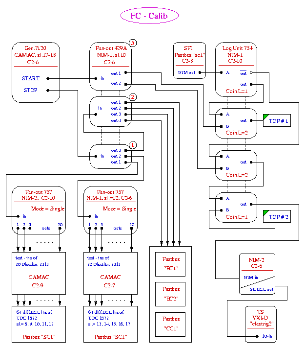
| 17 | Phillips 7120 | Precision Charge/Time Generator; FC Calibration STOP and START | |
| 18 | |||
| 19 | KineticSystems 3660 | Programmable Clock Generator; Clock for Phillips 7120 | |
| 20 | LeCroy 2313 | 16 Channel Programmable Discriminator, ECL | |
| 21 | LeCroy 2313 | 16 Channel Programmable Discriminator, ECL | |
| 22 | LeCroy 4418 | 16 Channel Programmable Logic Delay 32 Fan-Out, ECL | |
| 23 | LeCroy 4516 | 16 Channel 3-Fold Programmable Logic Unit, ECL | |
| 24 | KineticSystems 3922 | Parallel Bus Crate Controller | |
| 25 |
| VXI-D | 1 | MVME 2306 | Motorola's VME Processor Module |
| JLAB Clock Module | High MHz Clock for Level 1 Log.Modules; Two cables -> VXI-D (sl.9) | ||
| 2 | JLAB Logic Module | (5 Inputs / 1 Output) Level 1, Sector 1 | |
| 3 | JLAB Logic Module | (5 Inputs / 1 Output) Level 1, Sector 2 | |
| 4 | JLAB Logic Module | (5 Inputs / 1 Output) Level 1, Sector 3 | |
| 5 | JLAB Logic Module | (5 Inputs / 1 Output) Level 1, Sector 4 | |
| 6 | JLAB Logic Module | (5 Inputs / 1 Output) Level 1, Sector 5 | |
| 7 | JLAB Logic Module | (5 Inputs / 1 Output) Level 1, Sector 6 | |
| 8 | Event Processor | 6 Input Channels collect Outputs from 6 Sectors of Level 1 | |
| 9 | JLAB Clock Delay | Two delay cables -> VXI-D (sl.1: Clock Module) | |
| 10 | OR Module | 32 Input Channels (diffECL), VME Programmable | |
| 11 | JLAB RESET Board | VME Module in VME/VXI Adapter | |
| 12 | JLAB TS | Trigger Supervisor with 12 Independent Level-1 Inputs | |
| 13 | JLAB Converter | NIM/seECL/NIM | |
| JLAB Fan-out | diffECL Fan-out of 12 PRESCALED from TS |
| NIM 1 | 1 | Phillips 792 | Delay Module; Delay for ADC GATE |
| 2 | JLAB Delayed Fan-out | L1 ACCEPT -> ADC GATE and TDC START | |
| 3 | JLAB Fan-out | seECL -> 7 seECL; Fan-out of TDC START | |
| 4 | JLAB Fan-out | seECL -> 8 diffECL; Fan-out of ADC GATE | |
| 5 | Phillips 757 (octal) | Mixed Logic Unit; Inputs: EN, GO, BUSY from TS | |
| 6 | Phillips 726 | TTL/NIM/ECL Level Translator; Not used | |
| 7 | Phillips 726 | TTL/NIM/ECL Level Translator; for UNGATED Scaler | |
| 8 | LeCroy 4616 | ECL/NIM/ECL Converter; for RUNGATED Scaler | |
| 9 | LeCroy 4616 | ECL/NIM/ECL Converter; for LIVEGATED Scaler | |
| 10 | LeCroy 429A (4x4) | Logic Fan In/Out; Inputs: Calib. STOP/START, OR Module BUSY | |
| 11 | Phillips 706 | Leading Edge Discriminator; EC LASER, Helicity, Helicity-bar | |
| 12 | Phillips 757 (single) | Mixed Logic Unit; Fan-out of Calib. STOP from 7120 |
| NIM 2 | 1 | Phillips 726 | FE BUSY from FC (1-5) -> "OR" Module (VXI-D: "clastrig2")
HELICITY BITS (8&9) -> LD1 (14&15, VME: "scaler1") LEV-2 SECTOR BITS (11-16) -> LD2 (0-5, VME: "scaler1") |
| 2 | Phillips 794 (quad) | Gate/Delay Generator; FAST CLEAR and L1 ACC from TS, INHIBIT for TS and Delay for TDC START |
|
| 3 | JLAB Converter | NIM->seECL (2x4), seECL->NIM (2x4) | |
| 4 | Phillips 757 (octal) | Mixed Logic Unit; Mostly for HELICITY | |
| 5 | Phillips 726 | TTL/NIM/ECL; ECL Outputs: ASYNC.MOR.MISC -> FC Lev.3 | |
| 6 | Phillips 794 (3) | Gate/Delay Generator; Inverted HELICITY -> Counting Room | |
| 7 | JLAB Fan-out (12->A,B) |
A. PRESCALED from TS -> (0-11)
V560E (sl.7, VME: "scaler1") B. PRESCALED from TS -> (0-11) LD1 (sl.15, VME: "scaler1") |
|
| 8 | JLAB Fan-out (12->A,B) | Fan out of OR LEV-1 TRIG | |
| 9 | JLAB Clock Generator | 1 MHz, 100KHz, 10KHz, 1KHz | |
| 10 | JLAB Dual Converter | A. L1 ACCEPT, seECL -> diffECL B. HELICITY, NIM -> diffECL |
|
| 11 | JLAB Converter seECL/diffECL (2x16) |
OR LEV-1 TRIG, L1 ACCEPT and TS CLEAR -> "scaler1" | |
| 12 | JLAB Fan-out (seECL->8) | 4 seECL outputs (TS CLEAR) -> Space Frame 4 diffECL outputs (TS CLEAR) -> FC: SC1, CC1, EC1, EC2 |
| VME | 1 | MVME 2400 | Motorola's VME Processor Module |
| 2 | JLAB RESET Board | Remote Power Reset | |
| 3 | JLAB TI Board | VME Trigger Interface; BRANCH IN/OUT -> TS | |
| 4 | CAEN V560E | 16 Channel Scaler; No VETO, UNGATED | |
| 5 | CAEN V560E | 16 Channel Scaler; VETO = Inverted GO from TS, RUNGATED | |
| 6 | CAEN V560E | 16 Channel Scaler; VETO = TS BUSY or TS EN1, LIVEGATED | |
| 7 | CAEN V560E | 16 Channel Scaler; No VETO; (0-11) PRESCALED from TS, (12) L1 ACCEPT, (13) OR LEV-1 TRIG |
|
| 8 | CAEN V560E | 16-ch Scaler; No VETO; (0) L2 FAIL, (1) L2 PASS [copies to TS] (2) L2 START, (3) TS CLEAR, (4) L2 ACC, (5) L3 ACC [from TS] (8-15) from MLU2 (outputs:8-15, sl.17) |
|
| 9 | CAEN V560E | 16-ch Scaler; No VETO; (0-15) from MLU1 (outputs:0-15, sl.14) | |
| 10 | FT Optic Board | HELICITY, optic IN -> 2 NIM Outputs | |
| 11 | JLAB FLEXIO | Not used | |
| 12 | JLAB Converter, 5 sec. | Fan-out with Converter (seECL -> diffECL -> seECL) | |
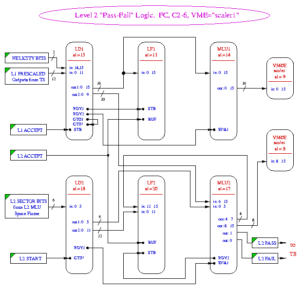
| 13 | JLAB LF1 |
VME Latch FIFO;
(0-15) In-1 <- LD1 (Out-1:0-15, sl.15) (Daisy-chain) In-2 -> MLU1 (inputs:0-15, sl.14) BUF <- L2 ACC, STB <- RDY1 from LD1 (sl.15) |
|
| 14 | JLAB MLU1 |
VME Memory Lookup Unit;
(0-15) Inputs <- LF1 (In-2, sl.13) (0-15) Outputs -> Scaler CAEN V560E (sl.9) ENA1 <- RDY2 from LD1 (sl.15) |
|
| 15 | JLAB LD1 |
VME Latch Driver;
(0-11) Inputs <- PRESCALED from TS (14&15) Inputs <- HELICITY BITS (0-15) Out-1 -> LF1 (In-1, sl.13) (0-9) Out-2 -> MLU2 (inputs:6-15, sl.17) RDY1 -> STB of LF1 (sl.13), RDY2 -> ENA1 of MLU1 (sl.14) STB <- L1 ACC from TS, GTO1=GTIN (joined by jupmers) |
|
| 17 | JLAB MLU2 |
VME Mem. Lookup Unit;
(0-5) Inputs <- LD2 (Out-1:0-5, sl.18) (6-15) Inputs <- LD1 (Out-2:0-9, sl.15) (0) Output -> L2 FAIL to TS (1) Output -> L2 PASS to TS (4-7) Outputs -> LF2 (In-2:12-15, sl.20) (8-15) Outputs -> Scaler CAEN V560E (inputs:8-15, sl.8) ENA1 <- RDY1 from LD2 (sl.18), RDY2 -> STB of LF2 (sl.20) |
|
| 18 | JLAB LD2 |
VME Latch Driver;
(0-5) Inputs <- L2 SECT.BITS from Lev2 MLU (0-5) Out-1 -> MLU2 (inputs:0-5, sl.17) (0-11) Out-2 -> LF2 (In-2:0-11, sl.20) RDY1 -> ENA1 of MLU2 (sl.17), GTIN <- L2 START from TS |
|
| 20 | JLAB LF2 |
VME Latch FIFO;
(0-11) In-2 <- LD2 (Out-2:0-11, sl.18) (12-15) In-2 <- MLU2 (outputs:4-7, sl.17) BUF <- L2 ACC, STB <- RDY2 from MLU2 (sl.17) |