| Home > Products > Scientific Instruments > DG535 | ||||
 |
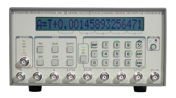
Digital Delay GeneratorDG535 — Digital delay / pulse generator (4 ch.) |
|||
|
||||
Features & Specifications
|
||||||||||||
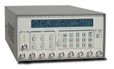
Delay OutputsThere are four delay output channels: A, B, C and D. The logic transitions of these outputs can be delayed from an internal or external trigger by up to 1000 seconds in 5 ps increments. The T0 pulse, which marks the beginning of a timing cycle, is generated by the trigger signal. The insertion delay between an external trigger and the T0 pulse is about 85 ns. Delays for each channel may be "linked" to T0 or any of the other delay channels. For instance, you can specify the delays of the four channels as: A = T0 + 0.00125000 Pulse OutputsIn addition to the four delay outputs, there are four pulse output
channels: AB, -AB, CD and -CD. The leading edge of the AB pulse
coincides with the leading edge of the earlier of A or B, and
the trailing edge of AB coincides with the leading edge of the
later of B or A. For instance, in the previous example, a 50 ns
pulse would appear at the AB output and a 1 ms pulse at CD. Pulses
as short as 4 ns (FWHM) can be generated in this manner. The complementary
outputs (-AB and -CD) provide a pulse with identical timing and
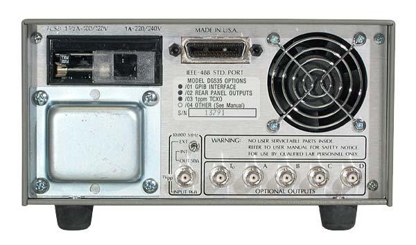
inverted amplitude. Each delay and pulse output has an independently adjustable offset and amplitude which can be set between -3 V and 4 V with 10 mV resolution. The maximum transition for each output is limited to 4 V. In addition, you can also separately select 50 Ω or high impedance termination for each output. Preset levels, corresponding to standard logic families, can also be selected. TTL, NIM and ECL levels can all be selected with a single key press. TriggeringThe DG535 can be triggered internally from 1 mHz to 1 MHz with four-digit frequency resolution. External, single-shot and burst mode triggers are also supported. For power control applications, the DG535 can be synchronized to the AC line. An optional trigger inhibit input allows you to enable or disable triggering with a TTL input signal. ±32 Volt OutputsFor applications requiring higher voltages, a rear-panel high voltage (±32 V) option is available. This option provides five rear-panel BNCs which output 1 µs pulses at the transition times of the front-panel T0, A, B, C and D outputs. The high voltage option does not affect the function or the timing of the front-panel outputs. The amplitude of the rear-panel outputs is approximately 8× the corresponding front-panel output, and the outputs are designed to drive 50 Ω loads. Since these outputs can only drive an average current of 0.8 mA, charging and discharging the cable capacitance may be the most important current limiting factor to consider when using them (assuming a high impedance load). In this case, the average current is: I = 2Vtf/Z, where V is the pulse step size, t is the length of the cable in time (5 ns per meter for RG-58), f is the pulse repetition rate, and Z is the cable's characteristic impedance (50 Ω for RG-58). Internal or External TimebaseBoth internal and external references may be used as the timebase for the DG535. The internal timebase can be either the standard 25 ppm crystal oscillator timebase, or the optional 1 ppm Temperature Compensated Crystal Oscillator (TCXO). The internal timebase is available as a 1 Vpp square wave on a rear-panel BNC. This output is capable of driving a 50 Ω load and can be used to provide a master timebase to other delay generators. Any external 10.0 MHz reference signal with a 1 Vpp amplitude can also be used as an external timebase. Easy to Use, Easy to ProgramAll instrument functions can be accessed through a simple, intuitive, menu-based interface. Delays can be entered with the numeric keypad in either fixed-point or exponential notation, or by using the cursor keys to select and change individual digits. The backlit 20-character LCD display makes it easy to view delay settings in all lighting conditions. The DG535 comes standard with a GPIB (IEEE-488) interface. All instrument functions can be queried and set via the interface. You can even display the characters the DG535 has received over the interface on the front-panel LCD display. This can be valuable when debugging programs which send commands to the instrument. DG535 Timing Diagram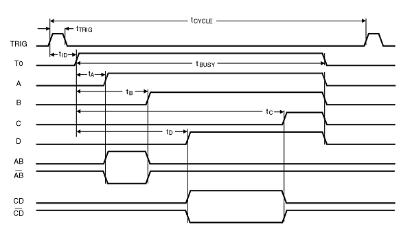 A timing cycle is initiated by an internal or external trigger. T0 is asserted approximately 85 ns after an external trigger. Outputs A, B, C and D are asserted relative to T0 after their programmed delays. All of the outputs return low about 800 ns after the longest delay. The pulse outputs, AB and CD, go high for the time interval between their corresponding delay channels.
|
||||||||||||
Specifications |
|||||
Delays |
|||||
| Channels | Four independent delay outputs | ||||
| Range | 0 to 999.999,999,999,995 seconds | ||||
| Resolution | 5 ps | ||||
| Accuracy | 1500 ps + timebase error × delay | ||||
| Timebase | Standard: 25 ppm crystal oscillator Optional: 1 ppm TCXO (opt. 03) External: 10.0 MHz reference input |
||||
| RMS jitter | <50 ps + 10-8
× delay (T0 to any output) <60 ps + 10-8 × delay (ext. trigger to any output) |
||||
| Trigger delay (typ.) | 85 ns (ext. trigger to T0 output) | ||||
External Trigger |
|||||
| Rate | DC to 1/(1 µs + longest delay) | ||||
| Threshold | ±2.56 VDC | ||||
| Resolution | 10 mV | ||||
| Slope | Trigger on rising or falling edge | ||||
| Impedance | 1 MΩ + 40 pF or 50 Ω | ||||
Internal Rate Generator |
|||||
| Rate | Single shot, 0.001 Hz to 1.000 MHz, or Line | ||||
| Resolution | Four digits, 0.001 Hz below 10 Hz | ||||
| Accuracy | Same as timebase | ||||
| Jitter | 1:10,000 | ||||
| Settling | <2 seconds for any rate change | ||||
| Burst mode | 2 to 32766 pulses per burst at integer multiples (4 to 32767) of the trigger period | ||||
Outputs |
|||||
| Load | 50 Ω or high impedance | ||||
| Rise time | 2 to 3 ns (typ.) | ||||
| Slew rate | 1 V/ns | ||||
| Overshoot | <100 mV + 10 % of pulse amplitude | ||||
| Levels | TTL: 0 to 4 VDC (normal or inverted) ECL: -1.8 to -0.8 VDC (normal or inverted) NIM: -0.8 to 0.0 VDC (normal or inverted) VAR: Adjustable offset and amplitude between -3 and +4 VDC with 10 mV resolution. 4 V maximum transition. |
||||
| Accuracy | ±(50 mV + 3 % of pulse amplitude) | ||||
| Option 02 | Rear panel 1 µs pulses corresponding to T0, A, B, C, D outputs with nominal amplitude of 8× the front-panel outputs at 1kHz rep rate. Output level reduced by 2 V/mA of additional average output current. | ||||
Fast Rise Time (opt. O4A) |
|||||
| Output amplitude | +0.5 to 2.0 VDC | ||||
| Output offset | -0.8 VDC (typ.) | ||||
| Transition time Rise (20/80 %) Fall (20/80 %) |
|
||||
| Pulse aberrations Foot Ring |
4 % (typ.) ±5 % (typ.) |
||||
Fast Fall Time (opt. O4B) |
|||||
| Output amplitude | -0.5 to -2.0 VDC | ||||
| Output offset | +0.8 VDC (typ.) | ||||
| Transition time Rise (20/80 %) Fall (20/80 %) |
2500 ps (max.) 100 ps (max.) |
||||
| Pulse aberrations Foot Ring |
4 % (typ.) ±5 % (typ.) |
||||
General |
|||||
| Display | Backlit 20-character LCD | ||||
| Computer interface | GPIB (IEEE-488). All instrument functions and settings may be controlled over the interface bus. Interface queue can be viewed from the front panel. | ||||
| Dimensions | 8.5" × 4.75" × 14" (WHL) | ||||
| Weight | 10 lbs. | ||||
| Power | 70 W, 100/120/220/240 VAC, 50/60 Hz | ||||
| Warranty | One year parts and labor on defects in materials and workmanship | ||||
|
Stanford Research Systems, Inc. • 1290-D Reamwood Ave., Sunnyvale, CA 94089 Phone: (408) 744-9040 • Fax: (408) 744-9049 • email: info@thinkSRS.com • www.thinkSRS.com © Stanford Research Systems, Inc. 2003 |